
Headlines of the Day
India must shift focus from chip project approvals to production, PHDCCI
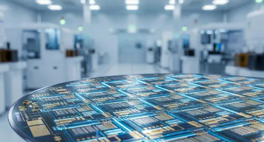
While India has successfully approved mega semiconductor projects, the current planned capacity will only meet a fraction of domestic consumption, necessitating an urgent shift of focus from project announcements to actual production, the PHD Chamber of Commerce and Industry (PHDCCI) said on Wednesday.
Speaking at the PHDCCI’s Semiconductor India 2026 national conference, Karan Mangla, Co-Chair of the Foreign Trade & Investment Committee at PHDCCI, cautioned that India’s domestic semiconductor market is on a trajectory to cross USD 100 billion by 2030, a demand that cannot be met with imported silicon.
“The union budget’s Rs 8,000 crore allocation and the launch of ISM 2.0 signal that our government understands this is a decade-long campaign, not a ribbon-cutting event. But as an industry practitioner, I have to be candid: Approvals are not chips. Announcements are not yield,” Mangla said.
He noted that even at full capacity, the currently approved fabrication plants (fabs) and OSATs will cover only a fraction of India’s consumption, with the rest still relying on imports.
Acknowledging that India has successfully moved from “intent to infrastructure”-with 12 projects worth about Rs 1.64 lakh crore approved across seven states, Micron’s Sanand facility operational, and Tata Electronics racing towards its first silicon in Dholera-Mangla said the next threshold is much harder.
“The mission has crossed the hardest threshold, believing it’s possible. The next threshold is harder: converting steel and silicon into shipped sub-volumes, quarter after quarter without excuses,” he said.
To bridge this gap, Mangla outlined a three-point roadmap for the manufacturing sector: speed in infrastructure, industrial-scale talent, and demand-side Commitments.
He stressed that every month of delay keeps downstream electronics, automotive, and defence manufacturers import-dependent.
On the talent front, he pointed out that while India commands roughly a fifth of the world’s chip design workforce, design talent does not automatically translate to fab and packaging talent. He estimated that India will need 300,000 trained semiconductor professionals over the next five to seven years, requiring academia and government to move at the industry’s pace.
Mangla urged Indian manufacturers in the telecom, automotive, and industrial sectors to deliberately commit to buying an “India-chip” early on, even if global alternatives are momentarily cheaper.
“Sovereignty is a shared discipline between the state that subsidises the fab and the industry that buys its output.”
He added that true self-reliance cannot be achieved by relying solely on large players alone.
Calling Micro, Small and Medium Enterprises (MSMEs) the “fourth pillar” of the journey, he said they are vital for building the daily component-level supply chain, including precision tooling and speciality chemicals.
The Union Cabinet on Wednesday cleared Rs 1.27 lakh crore for the second edition of the India Semiconductor Mission.
The government expects the new scheme to attract investments of around Rs 4 lakh crore and lead to semiconductor production worth Rs 2 lakh crore during the scheme period. The semiconductor programme builds on the first phase of the India Semiconductor Mission and will focus on six key areas â chip design, semiconductor equipment and materials, fabrication facilities, advanced packaging and testing, research and development, and talent development. PTI











You must be logged in to post a comment Login