
Headlines of the Day
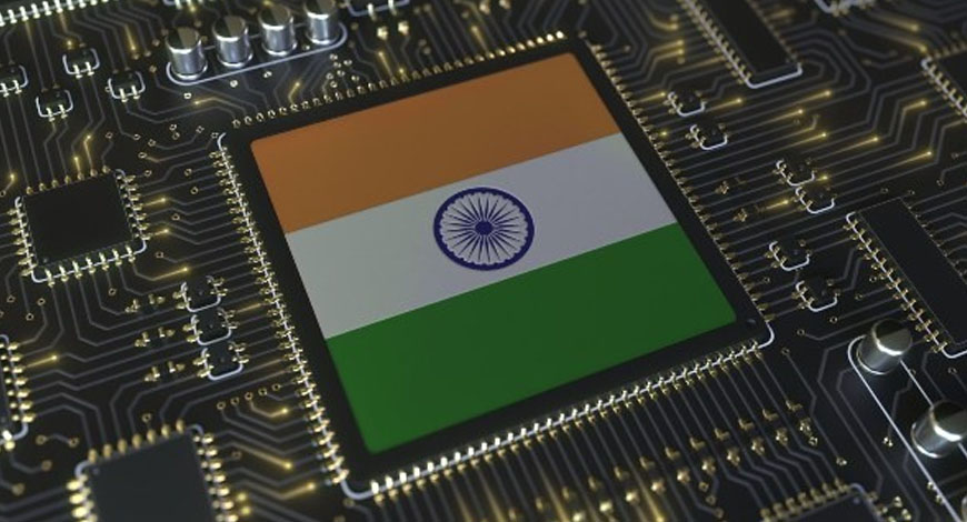
India Validation Center to boost semiconductor manufacturing
Ashwini Vaishnaw, Minister for Communications, Electronics & Information Technology on March 9 said the India Validation Center will help in developing manufacturing capabilities in the semiconductor sector.
The union railways, communications, electronics & IT minister commissioned the Applied Materials’ ‘India Validation Center’ in Bengaluru. The centre will enable end-to-end design, characterisation, and qualification of semiconductor equipment.
“This centre will further help develop manufacturing capabilities in the sector and exemplify the trust that global companies have placed in India,” Vaishnaw said.
India Validation Center proceeds the India Collaborative Engineering Center of Applied Materials, which will enable talent, and capability development for the semiconductor sector. It will also enable validation, process engineering, lab management, along with collaboration with academia and suppliers.
The Nasdaq-listed company Applied Materials is a materials engineering solutions provider, which is used to produce chip and advanced display.
Silicon wafers of 300-mm (around 12 inches) can be processed in the India Validation Center, which is being touted as the first by a private player in India.
“The envisaged semiconductor ecosystem is going to play a huge part in making India a developed nation. The India Validation Center is a testament to the dedication and effectiveness of our approach to build India’s resiliency in chip manufacturing,” said Vaishnaw, who is on a one-day visit to Bengaluru.
Vaishnaw said that almost every consumer tech product that runs on a chip today has Applied Materials engineering “imprinted” in them.
Prabu Raja, president of the semiconductor products group at Applied Materials said the company will continue to develop its capabilities in India. “(We will) support customers and work with supply chain partners to strengthen the local ecosystem and help India’s semiconductor industry.”
In an exclusive interview to Moneycontrol in Bengaluru, the minister said India’s next semiconductor programme will more significantly focus on the chip design ecosystem and aim to support the end-to-end production of at least 10 chipsets domestically, including design, fabrication and packaging.
Earlier in the day, Vaishnaw launched an indigenously built 2.4 tbps router, referring it as “a momentous achievement.” Moneycontrol


You must be logged in to post a comment Login