
Headlines of the Day
ICEA unveils seminal report on India’s semiconductor sector
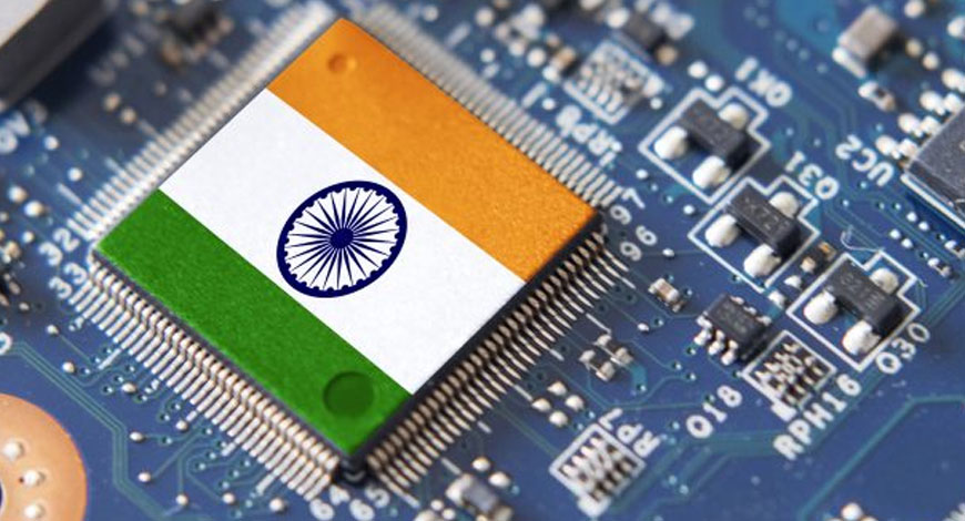
As India embarks on a significant venture to bolster its semiconductor manufacturing landscape, India Cellular & Electronics Association (ICEA) has released a groundbreaking report detailing the strategic roadmap and actionable recommendations for catapulting India to the forefront of the global semiconductor industry, specifically building semiconductor design and core IP creation in India. This report, a culmination of exhaustive research and expert consultations, sheds light on the challenges and opportunities facing India’s semiconductor sector against the backdrop of evolving global geopolitics.
Pankaj Mohindroo, Chairman of ICEA, articulates the report’s vision: “As we navigate through a transformative era in electronics manufacturing and hi-tech technology, India stands at a pivotal juncture to redefine its role in the semiconductor value chain. Our report is not just an analysis but a call to action for India to seize unprecedented opportunities and navigate challenges with strategic foresight.”
Key recommendations from the ICEA semiconductor report:
Fostering a robust design ecosystem: ICEA emphasizes the critical need to develop a holistic design ecosystem that encompasses the entire electronics value chain. This includes encouraging major Indian corporates and OEMs to delve into semiconductor design and core IP creation, thereby ensuring a vibrant domestic semiconductor design landscape.
Strategic support for semiconductor design firms: The report advocates for significant governmental and policy support, recommending the inclusion of mask sets in the Design Linked Incentive (DLI) scheme. Subsidizing the cost of mask sets by up to 80% for Indian design firms is proposed as a measure to facilitate the emergence of a strong Indian Intellectual Property Rights (IPR) framework.
Bridging the skill gap: Highlighting the acute need for skilled personnel in the semiconductor sector, ICEA calls for the development of industry-oriented curricula and comprehensive training programs. This initiative aims to equip the Indian workforce with the requisite skills to lead the country’s semiconductor revolution.
Enhanced funding mechanisms: The report underscores the importance of innovative funding approaches to support the semiconductor design ecosystem. This includes treating semiconductor chip design/manufacturing as a strategic sector, thereby enabling access to low-cost funds and establishing a dedicated capital market system for the electronics and high-tech industry.
Leveraging global opportunities: With the global shift in semiconductor manufacturing dynamics, particularly due to US sanctions on China, ICEA sees a strategic opportunity for India to advance into sub-14 nm technology nodes. The report suggests that India could leverage spare capacities, like TSMC’s for 7nm technologies, to accelerate its entry into advanced semiconductor manufacturing.
Investment in refurbished fab: Advocating for government investment in refurbished fabs, the report envisions supporting burgeoning semiconductor design firms and fostering a skilled semiconductor workforce as essential steps towards building a self-reliant semiconductor ecosystem.
“This report is a clarion call for unified action across government, industry, and academia to propel India into a leadership position in the global semiconductor arena,” Mohindroo concludes. “Together, we embark on a journey marked by innovation, self-reliance, and global competitiveness, poised to make India a semiconductor powerhouse.”
The ICEA report is a strategic document designed to capture and amplify the growth trajectory of India’s semiconductor industry, setting a course for India to not only participate but excel in the global electronics and semiconductor value chain.
The Union Cabinet’s recent approval for the establishment of semiconductor units marks a noteworthy advancement in the nation’s semiconductor industry. This initiative encompasses the setup of a semiconductor fabrication unit in Gujarat and two ATMP facilities, one in Gujarat and the other in Assam. These developments, part of the comprehensive ‘Development of Semiconductors and Display Manufacturing Ecosystems in India’ initiative, represent strategic steps toward enhancing India’s semiconductor manufacturing capabilities and affirm the nation’s commitment to securing a prominent position in the global semiconductor landscape.
For report, https://www.communicationstoday.co.in/the-challenges-opportunities-in-indian-semiconductor-industry-icea/
CT Bureau


You must be logged in to post a comment Login